Packaging technology is a technique that connects the bonding area of a chip with the external pins of the package and encapsulates it with an insulating material. In simpler terms, it is a technique for packaging integrated circuits. Taking the most common memory module as an example, what we see in terms of size and appearance is not the actual size and appearance of the memory, but rather a product that has been packaged (i.e., encapsulated) after the memory chip.
Qualified packaging can provide physical protection and standardized interconnectivity for the main product. With the rapid development of electronic technology, the requirements for small size, high density, and high-quality assembly are increasing. The integration of integrated circuits is increasing rapidly, and the heat generated by the chips is also increasing rapidly. If the packaging material cannot alleviate this problem, it is inevitable that the service life of the chip will decrease. This article briefly introduces several commonly used electronic packaging materials:
What are the performance requirements for qualified electronic packaging materials?
(1) Low coefficient of thermal expansion
(2) Excellent thermal conductivity
(3) Good airtightness, able to resist the extreme environment of high temperature, high humidity, corrosion, and radiation on electronic devices
(4) High strength and rigidity, can support and protect the inner chip
(5) Good processing and welding performance, to facilitate processing into complex shapes
(6) In the application of aerospace and other portable electronic devices, electronic packaging materials should have the characteristics of low density to reduce the weight of the device.
Several common electronic packaging materials are:
According to the materials used, semiconductor device packaging can be divided into metal packaging, ceramic packaging, and plastic packaging.
(1) Metal packaging:
Metal packaging is the most primitive form of semiconductor device packaging, with high mechanical strength, excellent heat dissipation performance, and good airtightness, unaffected by external environmental factors. The disadvantage is that it is expensive, inflexible in appearance, and cannot meet the rapidly developing needs of semiconductor devices. Traditional metal packaging materials include Cu, Al, Mo, W, Kovar, Invar, and W/Cu and Mo/Cu alloys.
(2) Plastic packaging:
Although the heat dissipation, heat resistance, and sealing properties of plastic packaging are inferior to those of ceramic packaging and metal packaging, plastic packaging has the advantages of low cost, thinness, simple process, and suitability for automated production. Its application range is extremely wide, from general consumer electronics products to precision ultra-high-speed computers. It is also the most widely used packaging method in the microelectronics industry.
The materials used in plastic packaging are mainly thermosetting plastics, including phenolic, polyester, epoxy, and organosilicon. Among them, epoxy resin is the most widely used but has poor airtightness and is sensitive to humidity. For example, in a humid environment, water vapor can cause corrosion and damage to the internal metal layer of the packaged device, and most of the transistors in plastic packaging contain lead, which is highly toxic.
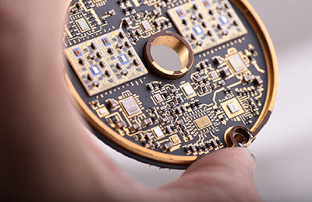
(3) Ceramic Packaging:
Ceramic is a hard and brittle material. Ceramic packaging is a hermetic packaging and is a main packaging technology for high-reliability applications. The main materials include alumina, beryllium oxide, and aluminum nitride.
Today's ceramic technology can control the size variation of sintering within a range of 0.1%. Multi-layer wiring structures with 30-60 layers can be made using thick film technology. Therefore, ceramics are also one of the main materials for manufacturing multi-chip module (MCM) packaging substrates.
Advantages:
1. In various IC component packaging, ceramic packaging can provide airtight sealing and protection for IC chips, making them highly reliable.
2. Ceramic is used as a material for IC chip packaging because of its extremely stable electrical, thermal, and mechanical properties, good corrosion resistance, high mechanical strength, small coefficient of thermal expansion, and high thermal conductivity. Its characteristics can be adjusted through the control of chemical composition and process. It can not only be used as a cover material for packaging, but also an important carrier substrate for various microelectronic products.
Disadvantages:
1. Compared with plastic packaging, it has a higher process temperature and cost.
2. Its ability for process automation and thin packaging is inferior to plastic packaging.
3. It has high brittleness and is prone to stress damage.
4. In packaging that requires low dielectric constants and high wiring density, it must compete with thin film packaging technology.
With the continuous improvement of the performance requirements of electronic products, ceramic packaging shells have been widely used in high-reliability and high-power electronic devices. The chip needs to be packaged in a shell that not only ensures mechanical protection and reliable sealing, but also has good conductivity and thermal conductivity to the outside world. This requires ceramics to be able to bond well with different metals, and the metallization process is a key process. Metallization refers to sintering or depositing a layer of metal on the ceramic so that the ceramic and metal can be joined together with high quality. The quality of metallization directly affects the hermeticity and strength of the packaging.
Due to the high technical barriers in the research and development and production of ceramic packaging, and the relatively high price of practical products, the coverage of its actual application areas still needs to consider cost reasons.
Declaration: This article is provided by CERADIR™ users or obtained from Internet, the content does not represent the position of CERADIR™. We are not responsible for the authenticity/accuracy of the article, especially the effects of the products concerned. This article is for study only, it does not constitute any investment or application advice. For reprinting, please contact the original author. If it involves the copyright and/or other issues, please contact us and we will deal with it asap! CERADIR™ has the interpretation of this declaration.