1. Manufacturing of photosensitive resistor porcelain
(1) Photoresistor porcelain
①Raw materials
When manufacturing photoresistors, CdS, CdSe and other Group II to VI compounds are generally used as raw materials. The raw materials must have extremely high purity. Generally, 5 9s (ie 99.999%) are required to strictly control harmful impurities. If the iron content reaches 0.001%, the sensitivity of the photoresist will be significantly reduced. Of course, the use of dopants must also pay great attention to purity.
The particle size of the raw material is also an important indicator. It should be ultra-fine powder to obtain good light guide performance. Generally, the particle size is in the range of 0.05 to 1 μm.
②Doping
There are two types of doping . One type is the donor dopant, with elements of group IIIA and VIIA. Such as Al, Ga, In and other trivalent metal compounds, NH4Cl4 and other halides. Another type of sensitizer (activator) is the acceptor dopant, with halides, sulfates, nitrates, etc. of group I and group V elements such as Cu, Ag, and Au.
A proper amount of Cu doping can improve the sensitivity of the photoconductor, but excessive Cu will make the performance of the photoconductor unstable. If the Cu doping amount exceeds 8X10⁻⁴, the performance of the photoconductor is unstable. The CI-doped CdS forms an n-type semiconductor, and the trap center formed by the acceptor Cu reduces the conductivity of the photoconductor. With the amount of Cu doping, the photoconductivity or brightness resistance of the photoconductor also changes. The appropriate amount of Cu doping can obtain a large dark and light resistance ratio.
③Flux
The melting point of CdS is 1750℃. In order to reduce the sintering temperature, flux must be added. Common fluxes are CdCl2, ZnCl2, NaCl, CaCl2, LiCI and other halides. The melting point of the flux should be lower than that of CdS, and it can melt at the sintering temperature to promote the sintering of CdS. For example, the melting point of CdCl2 is 568℃, and the firing temperature is higher than this temperature. However, the remaining CdCl2 during firing will slowly react with CdS and the electrode material In, which will affect the stability of the CdS photoresistor. For this reason, in the manufacturing process, the amount of CdCl2 needs to be strictly controlled, and the fired photosensitive sheet is washed in alkaline water before evaporating the electrode.
④ Dispersant
Although the flux can promote sintering, it will cause the CdS to form coarse crystals. The photoresistor and other light guide materials require fine crystals, so that the contact points between particles increase and the resistance increases, that is, the dark resistance is high, which is exactly what the photoresistor needs. The fine photoconductive powder used as photosensitive powder can also make the photosensitive layer uniform. The melting point of the dispersant is higher than the melting point of the flux, otherwise it will not function as a dispersant, and it is required to be soluble in water and not chemically react with the photoconductive powder in order to be washed off after firing.
Commonly used dispersants are NaF, Cal2, NaBr, CaBr2, NaCl, CaCl2, Na2SO4, CaCO3, Na2CO3, CaO, etc. Due to the different sintering temperatures of different materials, the same material can sometimes be used as a flux and sometimes as a dispersant.
Photoresistan
(2) Sintered film photosensitive resistor porcelain
① Cleaning of substrate
The sintered film photoresistor is to spray the prepared paste on the substrate with a spray gun, or print it on the substrate by screen printing. The physical and chemical properties of the substrate surface, the degree of surface smoothness, the degree of cleanliness, etc. The conductivity has a great influence, so the substrate must be cleaned. The cleaning method is to boil and wash with hydrochloric acid first. Then rinse with distilled water, add lotion to boil, and finally boil with deionized water repeatedly. In addition, there is ultrasonic cleaning in acetone or ethanol, and it is ready for use after drying.
② The preparation of slurry
The preparation process of sintered film photoresistor paste is listed in the table below
|
raw material |
purity |
Ratio(g) |
Preparation technology and function |
|
CdS |
Spectral purity |
2 |
Add appropriate amount of deionized water,porphyrization,drying |
|
CdSe |
Spectral purity |
0.5 |
Improve spectral response,Move it towards the long wave band,dark、Brightness resistance ratio increases,Faster response time;Calcined at 500℃ in N2 atmosphere before formula,Take out in 30min,Add deionized water,Research 、drying |
|
CaCl2 |
Analytically pure |
0.25 |
Add deionized water |
|
CuNO3 |
Analytically pure |
0.5mL |
Add the above three mixed materials to this solution, Grind uniformly |
③Sintering
The above mixed liquid is sprayed with a spray gun, dried, and placed in a tube furnace for firing. The firing atmosphere is a neutral nitrogen atmosphere, and the temperature is kept at about 600°C for a period of time and then cooled with the furnace to obtain the photosensitive resistance material.
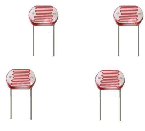
(3) Electrode for photoresistor
Photoresistor porcelain plus electrodes can be made into photoresistor. The ideal electrode is that there is no contact barrier between the electrode material and the photoconductor, and it is required that the electrode material does not chemically react with the photoconductor, and is not affected by changes in light, temperature or applied voltage.
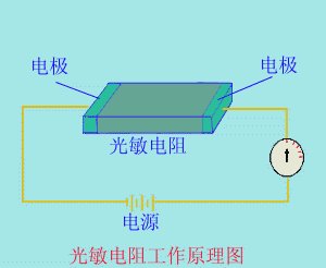
For n-type semiconductors, metal materials with a work function smaller than that of semiconductors should be selected as electrode materials; for p-type semiconductors, the opposite is true. Experiments have proved that for CdS and CdSe photoresistors, gold, silver, copper, carbon, and platinum are used as electrode materials, and ohmic contacts cannot be formed. Vacuum evaporation can be used to evaporate indium and gallium onto CdS and CdSe photoconductors , In order to achieve the purpose of ohmic contact. The melting point of indium is 155°C, and the melting point of gallium is only 29.8C, which are quite low. Therefore, the electrode can be made by the melting method. In the production process, indium tin alloy can also be used as an ohmic contact electrode.
Declaration: This article is provided by CERADIR™ users or obtained from Internet, the content does not represent the position of CERADIR™. We are not responsible for the authenticity/accuracy of the article, especially the effects of the products concerned. This article is for study only, it does not constitute any investment or application advice. For reprinting, please contact the original author. If it involves the copyright and/or other issues, please contact us and we will deal with it asap! CERADIR™ has the interpretation of this declaration.